Industrial CT Scanning PCBs
CT & X-Ray of PCBs
Industrial X-Ray & CT offer the ability to characterize the fine geometries of PCBs in ways other test methods cannot. From a simple visual inspection of solder joints using x-ray, to the calculation of those pores for surface area & volume using CT, these methods are used for everything from failure investigations, process change evaluations, and qualifications through sorting at Haven Metrology.
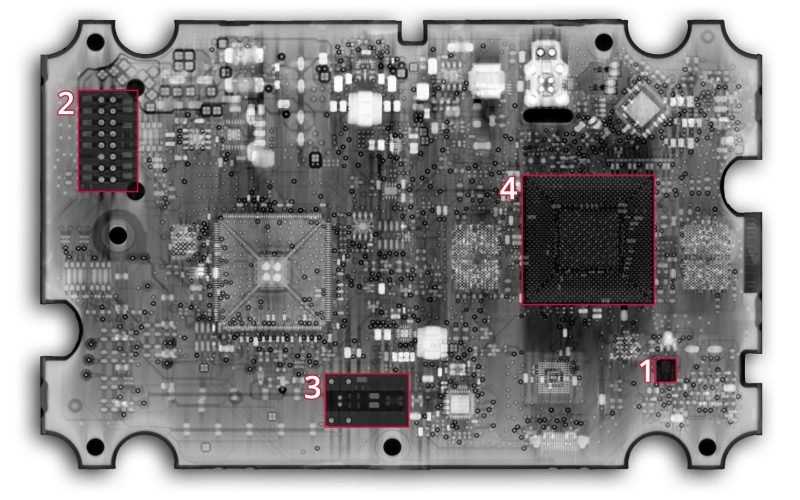
This case study highlights some of these techniques. We used a board with several types of components to demonstrate these capabilities. The PCB has been numbered to correspond with the high resolution images in the slideshow.

Image 1: Porosity in the pad is extracted. Typically we use porosity extraction to measure volumes in castings, but here we have used it to measure surface area. The large red void is .95mm2 corresponding with the deviation scale on the left.
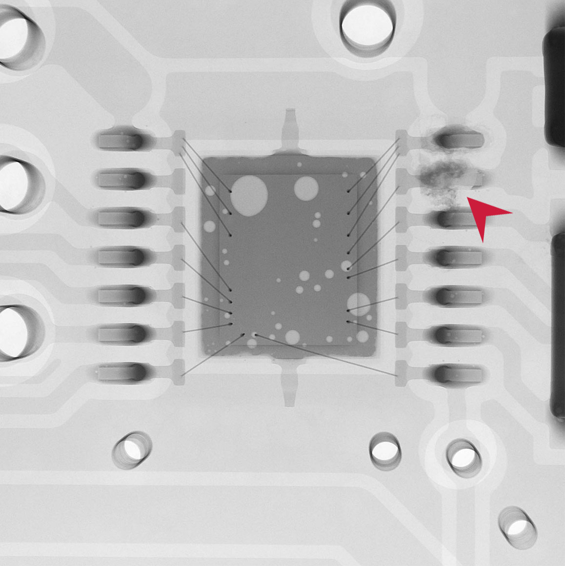
Image 2: Pin straightness, visual assessment of solder fill & porosity
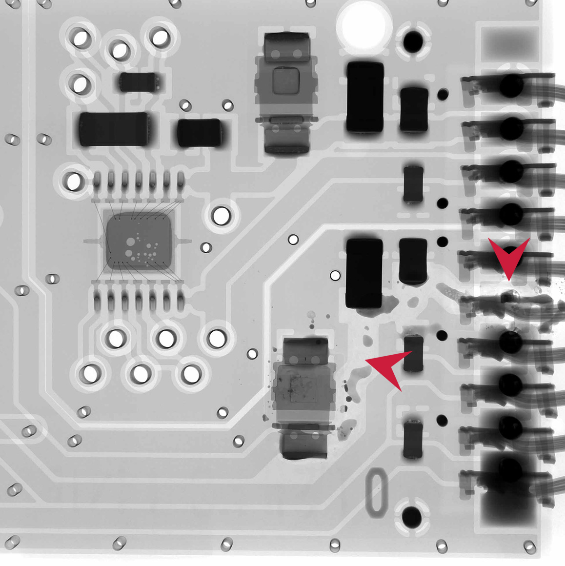
Image 3: Copper winding, capacitor integrity
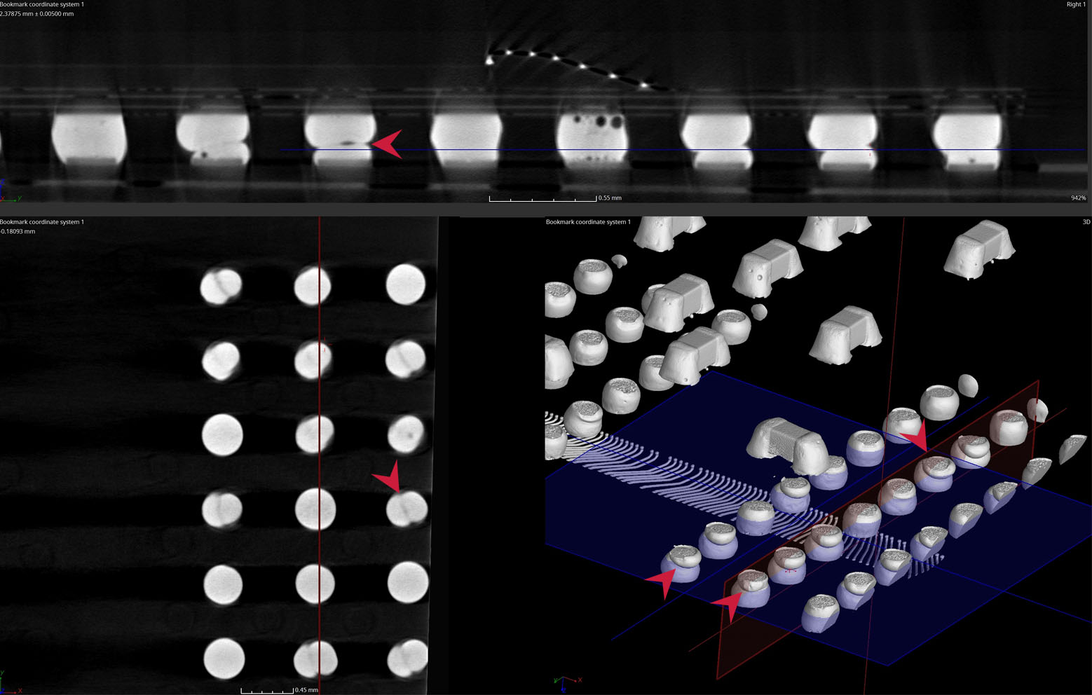
Image 4: BGA analysis for defects like popcorning, non-wetting (head in pillow), voiding, missing balls, misalignments, inconsistent standoff heights, and more.
High Resolution X-Ray of PCBs
X-Ray is used for the highest resolution imaging of PCBs. Because x-ray doesn’t require a 360 degree rotation of the component, we can place the component in close proximity to the x-ray source for the highest possible resolution. This allows us to detect the finest of foreign object debris, review all traces, and inspect all pore sizes.


BGA Defects
There are many types of BGA defects. Below is an image showing non-wetting / Head in Pillow. This is defined as the inability of the molten solder to form a bond with the base metal. It appears like a head on a pillow – two separate entities.


